| aaaaaaaa |

DPScope - Low-Cost USB Oscilloscopes
| |
| |
| |
| |
| | | | |
| Design Overview |
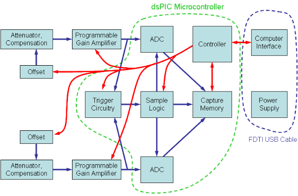
Below is a block diagram of the oscilloscope. The architecture is fairly traditional; the input signals are
conditioned in the analog frontend which depending on the signal levels either attenuates them or
amplifies them, and can also add offset. All this is necessary to make optimum use of the fixed voltage
range that the analog-to-digital converters can convert into digital information.
The analog-to-digital converters (ADCs) take the analog signals and convert them into digital numbers.
The sample logic controls the sampling process and the storage of the converted data in the capture
memory. The trigger circuitry decides when to start the sample process.
The controller takes care of setting signal gains and offset, setting up the sample logic, selecting trigger
source, trigger level, and trigger polarity, and communicating the the PC.
As you can see, the dsPIC30F2020 microcontroller allows to implement most of it without external circuitry
- controller, memory, sample logic, analog-to-digital converter (ADC), trigger and trigger level control all
reside within a single chip. This makes the design very compact, inexpensive, and easy to build.
The USB interface to the PC as well as the power supply for the scope are provided by FTDI's
serial-to-USB converter cable based on their FT232R device - again a very user-friendly solution since
there is nothing to assemble.
Click on the different tabs on the left side to get more information about particular parts of the design. You
find the full schematic in the download section.
| >> |
| << |
