| aaaaaaaa |

DPScope - Low-Cost USB Oscilloscopes
| |
| |
| |
| |
| | | | |
Input Stage / Analog Frontend (part 2)
| Click image to enlarge |
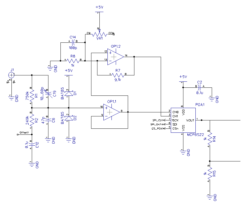
The two diodes (D1, D2) act as input protection, clipping any
signals to the preamplifier that exceed either +5V or 0V by more
than one diode drop. They need to be fast-switching (both in
conduction as well as in recovery) and have low input capacitance.
On the other hand, given the high input resistance value (750
kOhm) they don't need to shunt a lot of current even at large
overvoltages at the scope input.
inside the Microchip MCP6024). This buffering is also necessary because the following stage (the
MCP6S22 programmable-gain amplifier or PGA) does not react kindly to an input source with too high an
impedance - wild oscillations would be the result (yes, I tried and it is true!). The input divider's output
impedance (R1||R2) is around 187 kOhm while the PGA requires a source impedance of less than 1
kOhm.
The buffered signal drives one of the PGA's inputs (CH0) directly, and also feeds the input of a 1:10 gain
stage that produces a signal amplified by 10, which in turn goes to CH1 of the PGA. That way the PGA can
choose between less pre-amplification for large input signals, and large amplification for small signals.
The PGA has a specified bandwidth (not gain-bandwidth product!) of between 2 and 12 MHz (depending 5,
and 10 - according to my experiments higher settings (up to gain = 32 would be possible) are quite
sensitive and tend to exhibit excessive noise (an indication that oscillation may not be far away).
The MCP6024 has a gain-bandwidth product of 10 MHz, which is more than sufficient for the buffer stage
(gain = 1, so BW = 10 MHz), but marginal for the gain=10 stage (OP1.2) - we can only expect ~1 MHz of
bandwidth here, and the other stages (buffer stage, PGA, ADC inside the microcontroller) will further
reduce that number somewhat. For that reason I added C14 which increases the gain at higher
frequencies. It is chosen so that the gain increase starts approximately at the frequency where otherwise
the gain would start to drop off, that way the flat gain region is extended to higher frequencies. On my
prototypes I measured a gain-stage bandwidth of around 800 kHz without this compensation but almost
1.2 MHz with C14 in place - quite some bang (50% improvement) at virtually no cost! Its effect is also
clearly visible - much faster settling transitions - when using the scope to look at a fast-rising square
wave. Ideally C14 would be adjustable, but its value is not overly critical so I stuck with fixed 100pF which
was very close to the optimum I determined experimentally as well as by simulating the stage with
Microchip's free Spice tool. If C14 were too larger, overshoot would occur.
The resistor trimmer (VR1) is here to allow minor offset adjustments in the high-gain path. The main
reason for this is leakage current through the clamp diodes (D1, D2) which introduces a small positive
offset onto the signal. This offset is small, but becomes noticeable when multiplied by 10. (VR1 also
impacts the exact gain, but the effect is small enough to be ignored (less than 1%), especially when
compared to the tolerances of the gain-setting resistors (R7, R8).
| >> |
| << |
